Updated on June 7, 2011
June 1, 2011
I am going to post the first tip here about Printed circuit board ( PCB) etching. We all need to etch a PCB at some point .If you do it as much as I do you always look for faster ways . A few days ago I had to etch a breakout board for our developing rapid shaper/printer
I have been making circuit boards since I was a kid. I even remember making a circuit board with my mom’s hat glue and copper , and it worked!!! and very good that is .
So now that I am old (a little older …lol ) I use a little more profesional (still primitive) methods to make PCB’s. But I have to be honest ,nowadays there is such a saturation of PCB makers on the market from China , that is has to be a very special application before I will etch a board. It’s mostly for the R&D stages.
You can buy boards silkscreened, varnished with the whole works for a fraction of the price of what just the etching chemicals cost….None the less …why take the fun out of it right? I had this idea for some years now .I did a little researched on it , and found a few guys that does the exact same thing here : http://grandahl.net/feed/?p=19
So lets dive right in and discuss how I did it( and still developing it) :
What you need in this method:
To make a printed circuit board (PCB) you need a copper clad (one or 2 sided) fibreglass or phenolic copper board , a mask of some kind and an etching solution, its thats it simple, really it is!
So lets break it up sequentially:
1-The copper layered board , single or double sided
There is a slew of them online, just google all kinds of electronics and surplus supliers, I am not gonna get into that here.
2- The Masking
We will plot/scribe our mask straight to our PCB with a small little A4 Penplotter ,Like the HP7475A (get them on ebay for $50(US)). So why a penplotter?…..After years of etching I find myself more and more impatient. I want to draw the schematic on Cad or EAGLE , etch it and silkscreen or plot the component side all in 30 min. Yes it can be done that qiuck. Here is video plotting the pcb.
http://www.youtube.com/watch?v=IG9KNDvoRl4
It’s plotting straight on pc board in 5 min and ready to be etched (No photo sensitive exposing process etc.) . Use your favorite cad program export in HPGL (Hewlett Packard Graphic Language) and print/plot.
3- The etching
Various chemicals can be used ,I like ferric chloride acid, available everywhere,but yesterday I ran accross this link wich I will definitely try next time.Its cheap and readily available. Just be very carefull not blow yourself up in the process,read the whole post and comments carefully. … WARNING!!: …We take no responsibility for any of these formulations, use it at your own risk,discretion and common sense!!!…And DISPOSE of the acid in a proper legal way!!!
4-Plotting the component side
After etching ,the board can be re-inserted into the plotter.This time with the component side up and re plotted with all the colors of your choice. Now plot all components ,names and revision notes on top. .Thats about it.
Happy plotting/etching……TJ.
Links:
http://forums.reprap.org/read.php?184,4215
http://www.technick.net/public/code/cp_dpage.php?aiocp_dp=guide_pcb
June6, 2011
We expanded on our research and development on the plotter-etching method this weekend .And with a lot of hard work and dedication we had a good breakthrough!! . Here at CemShapes we go through all the grunt and pitfalls so you dont have to be aggravated with it. We will only extract the best and provide you with the right techniques and information to make you life easier . ( without breaking the bank.) And as always ” opensource is our motto ” so you will also know about all our mistakes and how we correct them.
Before this weekend we had no consistency in the final etchings (some came out good, some bad). The pen plotting straight to the PCB was not satisfactory yet. See Fig. 1 , for some of the bad etchings .
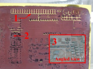
FIG 1, #1-Shows bad masking ,#2- shows deteriorated mask, #3- Angled view, Got a lot of bad etches like these while experimenting with many different pens and paints , Many times it worked but not consistent enough.
The acid breaks down/deteriorate the ink and paint masks before the etching is properly done. This was mostly due to the thin ink deposit on the boards. , Sorry , ….not consistent enough for success!
After Dozens of etchings I stopped and analized each board. I regrouped , brainstormed and took a whole new aproach. Right of the bat,this new method worked great, and it only took a few tries to perfect this method . And here is the best part …..We need no ink pens!! that can get dry!!!! ,only a scribe pen. Wich means you are ready to etch at any time!! .The new method is also just as quick and involves a thin coat of black spraypaint from a can for the mask, and scribed trace outline from the pen plotter. Explained here , step by step :
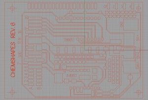
The cad drawing does need a few more curves or lines to create , but this by far outweighs the clogging of the plotter pens.( wich is a big pain after a few weeks of no plotting).The scribe is ready to go 24/7 …I LOVE IT!!! Here is the cad drawing in RHINOCEROS 5
1- THE PEN SCRIBE…. I used a regular felt tip plotter pen to make a steel scribe.
(A)…Remove the top inkplug.
(B)….Remove the fibre core ink container inside and push the felt tip out of the pen.Wash with soap.
(C)….use the shank of a drill bit a few thousands of a inch bigger in diameter than that of the felt tip inside the pen (this is for a nice tight fit in the plastic pen housing) , Sharpen to a 60 degree cone point ( very sharp tip) .
(D)….Push the cone sharpened drill shank into plastic pen housing and thats it!! it took me two minutes! and $1 for a 3mm drill bit.
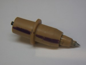
Fig 2. The modified plotter pen to a SCRIBER. Shown with the sharpened drill inside where the felt tip used to be..The line is for the same pen insertion/orientation every time.
.Because I only scribed once per curve , some traces did’nt get isolated because of paint burrs that got stuck in the grooves.So here is one more important tip when plotting:…scribed each otline twice. The way I did that was simply copy and paste the drawing right on top itself one time. That way you do a double plot without having to re-register your paper , It is the quickest and most accurate way to get a double scribeline. Also make sure the outline is one polygon all in one direction.This eliminates open corners.
IMPORTANT:…After scribing dont wipe of any paint burs. Leave them as is, otherwise you’ll push them back in the grooves,remember the scribeline is only about 0.1mm or so thick
2-PREPPING THE PCB… (A) Cut the PCB About 12mm oversize than your plot outline…. (B) Sand clean and get all tarnish off with 220 or 400 grit sandpaper so the paint have “teeth” to grip onto. Important: after sanding, wipe clean with acetone…. (C) Spray just one thin layer of paint to cover the whole board with enamel spraypaint. I used RUSTOLEUM OIL GLOSS BLACK , but any oil brand can be used. While waiting to dry (tack free in about 5 min) go to step 3 .
3- Plotting the A4 Paper …. (A) Use a thick piece of paper (photograph thickness or poster board) . The plotter moves pretty rapidly and the thin paper sometimes bend a little when changing Y-AXIS directions. Do a position plot with a regular pen or pencil . Leave the paper in the plotter …. (B) Tape your PCB right over that plot so it sticks over on all 4 sides about 6mm. …You are ready to scribe.
4-Plot/Scribing…… Scribe at a really slow speed ( on autocad the pen speed is 4 , I think it is 4cm / sec.) and make sure you do it twice on every curve or line and leave the paint burrs alone , just give a light blow of air to blow them off the board.
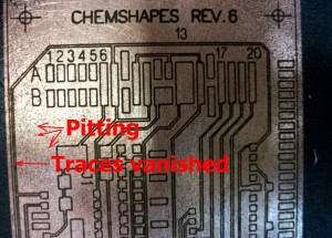
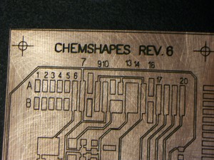
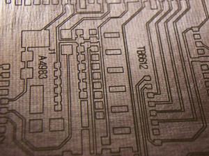
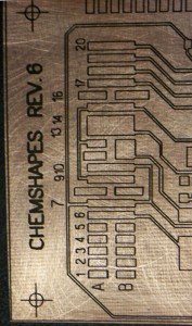
Fig 3.The first scribed board etching -First off ,I used an (already used)old acid mixture,the mask deteriorate and and some traces etched away and also pitted the copper cladding bad!
5-The etchant…… I used a “new” formula , 50/50 by volume …One volume unit of MURIATIC ACID(31.35% concentrate) @ $5/Gal. and one volume unit of HYDROGEN PEROXIDE (20% concentrate)@ $3/bottle . The MURIATIC you get at the pool and hardware supply and the PEROXIDE at a salon /beauty supply store.
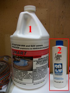
Fig 4, #1-MURIATIC acid (31.45% concentrate) (VERY CORROSIVE!) for pools,... #2-HYDROGEN PEROXIDE (20% concentrate) available at salon suplies
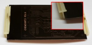
6- Etching process……When the board is ready to be etched move the whole process outside for good ventilation. add the plastic stand-off clips (See FIG 5. ) to the side to elevate the board of the contaner bottom . Have a second container ready with fresh water to rinse imediately. Add the MURIATIC ACID to the PEROXIDE in a flat container of your choice. Swirl for a few seconds to get homogenous and lower the board in the mixture …SLOWLY!!!..I did mine trace down,but trace up work just as good, this way no bubbles get trapped under it . Use a pencil and fan the PCB up and down in the mixture slowly to agitate the mixture even more.This also keeps good flow over the board to wash off the etched copper on top.
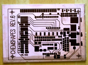
NOTE: THIS IS THE MOST AGRESSIVE ETCHANT SOLUTION I HAVE EVER EXPERIENCED BE CAREFULL IT IS EXTREMELY CORROSIVE!…. Watch your board being etched in 2 to 4 minutes (pending on your copper clad thickness). As it bubbles and activates you literally see the copper being washed of the PCB like fine dust. As soon as you see through the board,take out imediately and rinse of with fresh water. …..Believe me every second count…. its actually so fast its funny to watch …lol
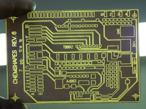
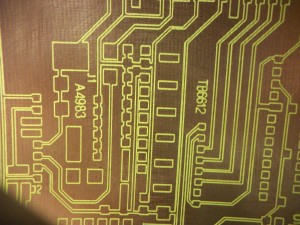
With a backlight...., nice and clean.... (the backlight diffracton makes the traces disapear in this picture). It does show how clean that tiny little scribe line can etch.
7-SAFETY
(A) It is a always a good idea to have a neutralizer like baking soda and extra water handy for your eyes and skin….
(B) wear glasses and nitrile gloves ,This is nasty stuff!! and extremely corrosive!!!….
(C) Even though you can use this mixture more than once , it looses it’s effectiveness after the first etch. It turns green into copper chloride , and the second time it takes too long to etch and the mask starts to deteriorate. I also don’t have the time and patience to sit there and stare at the PCB for 30 min……
(D) Dispose off properly(Definitely not into the kitchen sink or any plumbing for that matter) also I don’t like to store this mixture, I think it’s very unstable,so I use it only one time (it’s cheap enough)….
(E) Use your brain and COMMON SENSE when you do this kinda stuff and keep kids and pets away!!!…far away!!!
Till next time!!! Happy etch’n
TJ.
Recent Comments